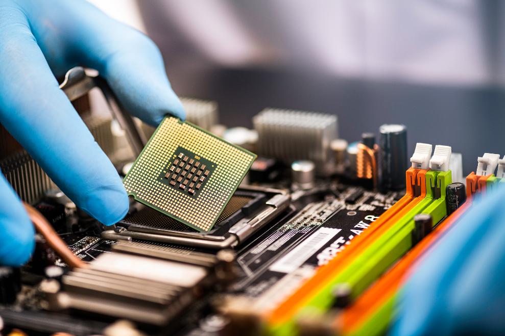
Semiconductors play a vital role in powering almost everything we use in our daily lives. They are found in smartphones, medical devices, cars, kitchen appliances, building automation systems, TV’s, computers and much much more. A semiconductor is a material product usually comprised of silicon or geranium, which conducts electricity more than an insulator, such as glass, but less than a pure conductor, such as copper or aluminum. Their conductivity and other properties can be altered with the introduction of impurities, called doping, to meet the specific needs of the electronic component in which it resides. With many of these chips comparable to the size of a fingernail, they are the most complex products on the planet.
The semiconductor industry is considered to be highly cyclical and is subject to periodic booms and busts and it is well known there is currently a worldwide shortage in semiconductors. As these global issues persist, the construction spend on new semiconductor plants is expected to push to €120 billion in the near future. The construction of a semiconductor factory, or fab, is highly complex and a massive undertaking so this article will look to highlight some of the important considerations to take into account.
-
What does it take to build a semiconductor factory?
A typical large, state of the art, semiconductor factory takes approximately 3 years to build, involving 6,000 construction workers and costing around €5.5 billion to complete. Some interesting numbers on what’s required for a large build (source Intel)
- At least 250,000 square feet – 4 american football fields could fit inside the clean room
- 600,000 cubic meters of concrete to be poured and 75,000 tons of steel reinforcement. This represents 2x the amount used to build the Burj Khalifa in Dubai, the world’s tallest building
- 35,000 tons of structural steel to be erected – 5x the weight of the Eiffel tower
- More than 1 million cubic meters of soil and rock to be removed – Equivalent to 400 Olympic-size swimming pools
- 9 million metres of cable to be installed – a distance equal to 214 full marathons.
An important first step is to realise the scope of the whole project and use effective pre-construction planning long before ground has been broken to mitigate against the impact of changes once started. Utilising Building Information Modelling (BIM) is a consideration that can help to improve the design and construction process from the outset.
-
Using the right construction management software
It goes without saying there is a huge amount of moving parts and critical steps at the different stages in the construction of a ‘fab’ build. A complex build requires the coordination of a host of contractors and suppliers, each with specific capabilities and permissions. Many contractor activities will be interdependent, with each step needing to be signed off by the relevant authority before work can commence on the next phase.
Therefore a consideration should be made for investing in a construction management software that is tailored specifically to your needs addressing both basebuild and tool installation, switching from a system turnover based solution to tool startup. This is where the EIDA construction project management platform excels and allows for real-time collaboration, streamlined document sharing, accurate budgeting amongst other key benefits.
-
Community & Environmental impact
When planning the construction of a new semiconductor facility, it is important to consider and evaluate the impact it will have on the surrounding community in order to minimise any potential environmental or public safety risks. For example, the construction of a fab can cause noise pollution, lost business revenue and traffic delays and can have an adverse effect on the local community and businesses in the area.
It is worth considering and determining the most efficient and effective ways to minimise the impacts of the construction process to the community during construction and even after the project is completed and manufacturing has started. Co-operation and communication with local government, development agencies and other important stakeholders is key to highlight the potential issues and make a plan to combat them.
There are also plenty of ways to mitigate the environmental impact of construction that should be considered including reducing fuel consumption, reducing noise pollution, reducing waste generation, minising the discharge of contaminants and utilising reusable technology. Many facilities are looking for better ways to be environmentally friendly both in construction and in day to day manufacturing. The new Infineon Technologies’ fab at Villach, Austria is one of the most environmentally advanced with around 80% of the site’s heating being generated by recycling waste heat; a feature that will save around 20,000 tons of CO2 every year. It shows what can be done.
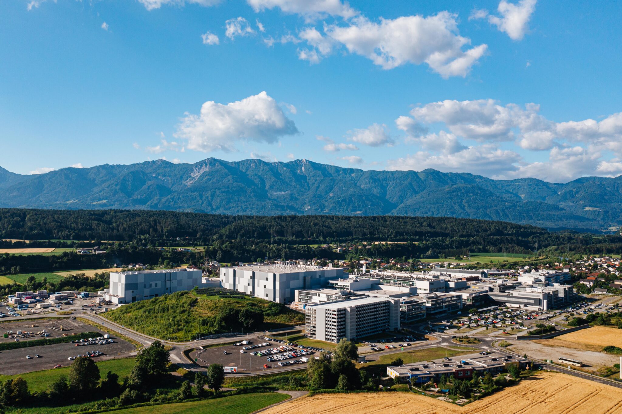
Infineon semiconductor plant in Villach, Austria
In conclusion, there are a whole host of considerations to take into account when planning to build a new semiconductor factory. By understanding the scope, scale and requirements of the project, choosing the right construction management software and by considering the environmental and community impact you will set yourself up for better delivery and success.
Speak to one of our senior consultants to find out how EIDA’s custom platform can improve the structure and flow of your projects, reducing risk and improving quality, build after build.