Reducing Risk and Increasing Accuracy in Semiconductor Builds
Semiconductor builds are some of the most complex, high-stakes construction projects in the world with multi-billion euro facilities, hundreds of contractors on site and millions of documents with little tolerance for documentation errors. So how do the best project teams keep it all under control? More and more, it comes down to how they manage their data.
In a semiconductor build, risk doesn’t usually arrive in one big moment, it creeps in over time. A vendor submittal gets reviewed against the wrong revision. A punch item gets closed out without the right sign-offs. A commissioning team shows up to start work and the documentation they need isn’t ready. Each of these feels manageable in isolation, but stack them up across a project with dozens of systems and hundreds of contractors, and you’ve got a genuine compounding problem.
The root cause is almost always the same, information is scattered, access is inconsistent, and there’s no single source of truth everyone can rely on. That’s exactly the problem EIDA can solve.
EIDA is a purpose built construction management, commissioning and turnover platform that covers the full project lifecycle from pre-construction design and vendor documentation right through to commissioning, qualification, and final turnover. The key word there is full. A lot of tools handle one part of the job well whereas EIDA connects all of them.
On semiconductor builds specifically, this matters because the handoffs between phases are where things tend to go wrong. Design data should be accurate before construction starts. Construction records should be complete before commissioning can begin. Commissioning documentation should be verified before handover. EIDA keeps all of that data connected, current, and accessible so the baton actually gets passed cleanly.
One of the most consistent sources of error on large builds is document control or more accurately, the lack of it. Multiple versions of drawings in circulation, submittals that haven’t been formally reviewed, test records that are filed in someone’s inbox rather than the project system.
EIDA’s Document Control module tackles this head on. Every document from contractor submittals, vendor submittals, engineering packages, test records, weld records lives in the platform, linked directly to the relevant system or equipment. Version control is enforced so you can’t accidentally work from an old revision because the current one is always right there. And because everything is linked to specific systems, there’s no hunting around to figure out what documentation applies where.
The result is super traceability with a full, auditable record of every document, every action, every approval, at any point in the project. If you need to find something six months later, it’s there.
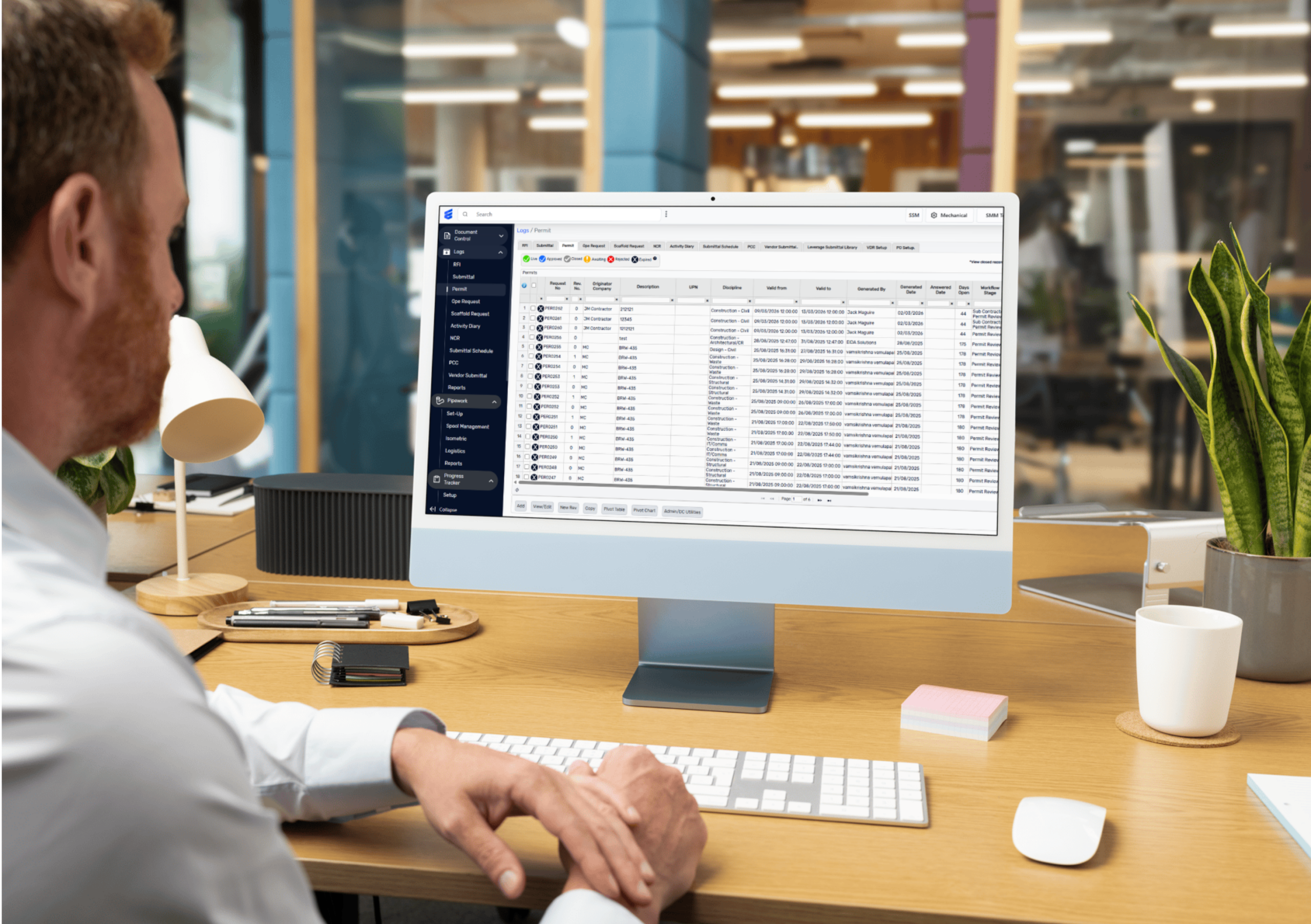
EIDA’s Quality Assurance module means quality checks aren’t an afterthought bolted on at the end, they’re embedded in the day to day workflow. Customisable checklists ensure that every inspection and test procedure follows the right steps. Punch items, those lists of outstanding defects and incomplete work that every project accumulates are tracked in real time, with clear ownership and sign off requirements. Nothing gets marked complete until it actually is.
All actions within EIDA carry a built-in audit trail. Every review, every approval, every closure is timestamped and logged. For semiconductor builds where regulatory compliance is so important, that kind of verifiable record is essential.
A semiconductor build also doesn’t just happen on site. Equipment is being manufactured, tested, and documented in facilities all over the world. Managing that vendor documentation like making sure Factory Acceptance Testing (FAT) records, material certificates, and operating manuals are all in order before equipment lands on site is a huge job in itself.
EIDA’s Vendor Documentation module and VTOP (Vendor Turnover Package) functionality bring that process into the same platform as everything else. Vendor submittals are tracked, reviewed, and approved within EIDA, with automated notifications keeping the process moving. By the time equipment arrives on site, the documentation has already been through the right reviews. No scramble to chase down certificates at the last minute.
Ask any commissioning manager what their biggest headache is, and they’ll tell you it’s starting work without the information they need. Incomplete pre-commissioning records. Systems that haven’t been formally accepted. Documentation that’s still with the construction team.
EIDA’s commissioning suite addresses this directly. The Systems Startup Matrix gives a clear, real-time view of which systems are ready to commission and which aren’t. C&Q (Commissioning and Qualification) workflows support GDP-compliant documentation and because all the construction data feeds directly into commissioning, teams can actually see the status of the work they’re taking over, rather than having to take someone’s word for it.
The Engineering Turnover Package (ETOP) and System Turnover functionality mean that when it’s time to hand over a system, the package is generated from the data that’s already in the platform. There’s no manually compiling documents from different sources and no missing sign offs. Just a clean, complete handover.
One of EIDA’s most practically useful features is the Tracker, a highly configurable tool that gives project teams a live view of progress across whatever they need to track. Equipment delivery and installation, documentation status, structural steel, cable installation, if it’s happening on the project, the Tracker can reflect it.
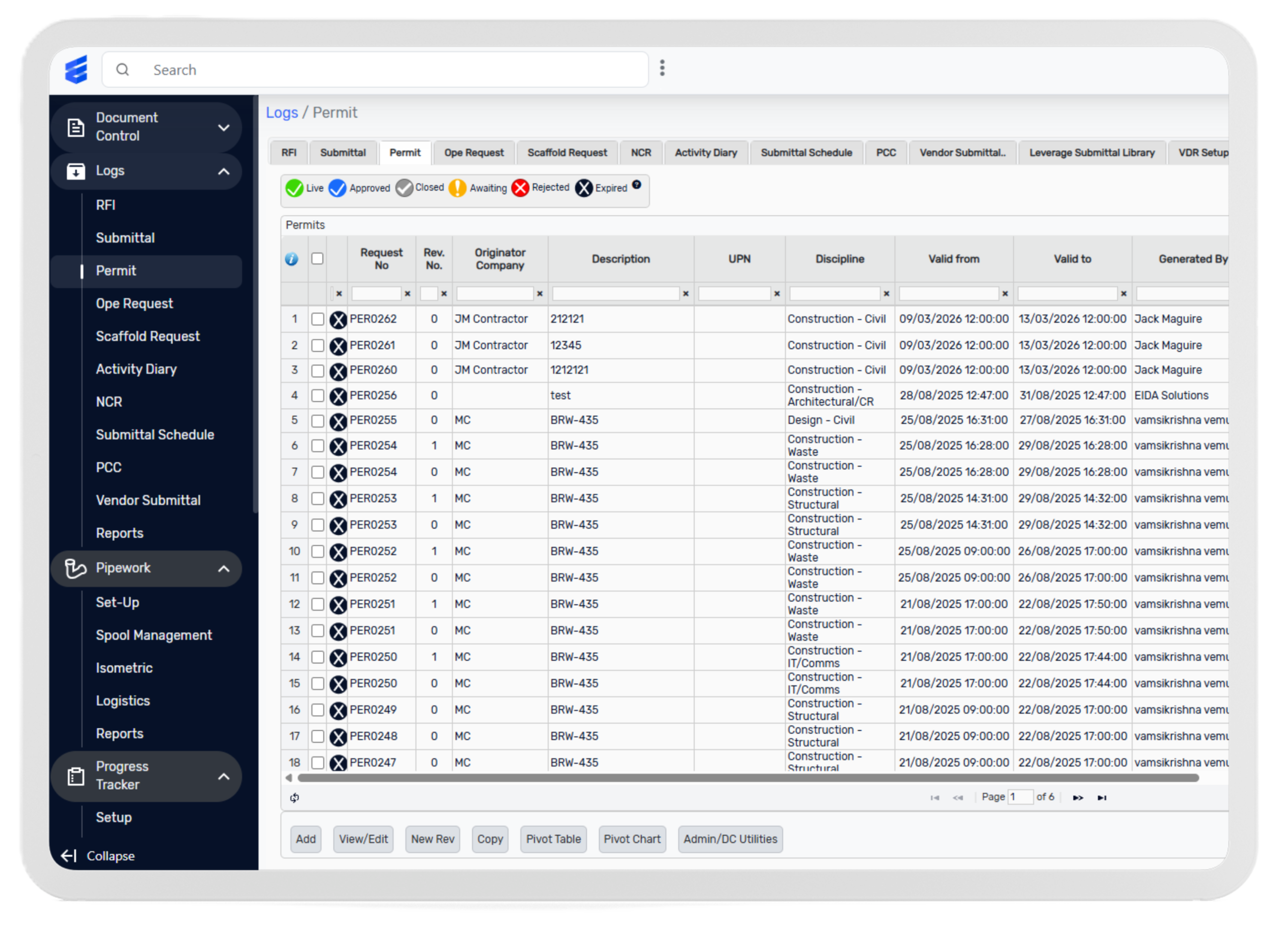
Combined with EIDA’s KPI dashboards and role based access controls (so everyone sees what’s relevant to them, and no more), project managers and site leads have a genuinely accurate picture of where things stand at any given moment. That means decisions get made on real data rather than status update meetings and manual spreadsheets.
EIDA has been deployed on some of the biggest semiconductor builds in the world, including a €2.3 billion plant in Ireland, a €1.6 billion expansion in Austria and the new €2.6 billion fab in India. These aren’t pilot projects, they’re full scale implementations on some of the most demanding construction projects in the world.
That experience shapes the platform and EIDA understands that semiconductor builds have particular requirements around the complexity of tool installation alongside base build, the regulatory demands and the sheer volume of documentation involved. The platform handles it.
Reducing risk on a semiconductor build ultimately comes down to one thing and that’s making sure the right information is available, accurate, and accessible to the right people at the right time. When that’s in place, errors get caught early, handoffs happen cleanly, and commissioning teams can actually do their jobs without fighting their way through incomplete documentation.
Want to see how EIDA works on a semiconductor build? Request a demo and talk to a senior consultant.